

HF87711_VC1/HF87711Q_VC1
Multi-Channel PCM 768KHz/DSD512 USB HiFi Codec Supporting USB/I2S/2CH SPDIF Input and Output plus Microphone Input
1. Introduction
1.1 Product Description
HF87711_VC1/HF87711Q_VC1 is a USB multi-channel and multi-interface HiFi audio codec supporting up to PCM 768KHz/DSD512, specifically designed for HiFi audio decoding and microphone recording applications.
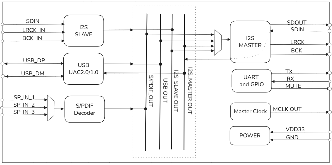
HF87711_VC1/HF87711Q_VC1 supports various standard audio formats, including USB Audio Class 1.0/2.0, S/PDIF, and I2S interfaces. The flexible audio interfaces allow HF87711_VC1/HF87711Q_VC1 to connect to various audio data converters, digital audio receivers and transmitters, and digital signal processors.
Compatible with AES3, S/PDIF, IEC 60958, and EIAJ CP-1201 digital audio interfaces.
HF87711_VC1/HF87711Q_VC1 provides multiple input and output modes, including USB input/I2S output, S/PDIF input/I2S output, I2S (slave) input/I2S (master) output, USB input/S/PDIF output, and USB microphone input, meeting the requirements of different application scenarios.
Important Notice
The HF87711Q_VC1 model supports MQA audio decoding, while the HF87711_VC1 model does not support this feature.
1.2 Product Features
Audio Performance Features
- Supports input and output sampling rates up to 768kHz
- Supports DSD64/128/256/512 formats
- HF87711Q_VC1 supports MQA decoding
- Built-in SSRC and ASRC modules, supporting conversion between different interfaces and different sampling rates
- Supports 16-32bit audio data formats
- Supports 2-channel S/PDIF input/output
- Supports microphone input
Interface Support Features
- Multiple Digital Interface Support
- Supports USB audio input/output
- Supports I2S slave mode audio input
- Supports I2S master mode audio output
- Supports S/PDIF audio input/output
- Supports UART configuration interface
- Supports microphone input interface
USB Functional Features
- USB Interface Features
- Supports UAC 1.0
- Supports UAC 2.0
- Supports firmware upgrade via USB
- Supports HID, can upgrade MCU firmware via HID
- Supports UAC 1.0 microphone input
System Compatibility - UAC 2.0 protocol, supports ASIO - Supports multiple operating systems such as Windows, Linux, Android, macOS, and iOS
1.3 Application Scenarios
- USB HiFi Decoder
- USB HiFi Audio Interface
- USB HiFi Digital Player
- USB HiFi Microphone Recording Device
1.4 Product Functional Block Diagram
1.5 Ordering Information
| PRODUCT | ORDERING NUMBER | PACKAGE BODY | SIZE (NOM) | Hardware Model | Comments |
|---|---|---|---|---|---|
| HF87711_VC1 | HF87711-VC1 | SMT LGA-52 | 13x13mm | A316-Mini-V1 | |
| HF87711Q_VC1 | HF87711Q-VC1 | SMT LGA-52 | 13x13mm | A316-Mini-V1 | Supports MQA Decoding |
2. Modes and Specifications
2.1 Supported Input/Output Modes
| Mode Number | Input/Output Mode | Description | Mode Switching Command Value (Refer to Product Configuration Protocol Commands 0x03 and 0x23) |
|---|---|---|---|
| 1 | USB(UAC2.0) in-I2S(Master) out | USB input, I2S output, UAC2.0 | 0x00, 0x80, 0xa9, 0x00, 0x01 |
| 2 | USB(UAC1.0) in-I2S(Master) out | USB input, I2S output, UAC1.0 | 0x00, 0x80, 0x01, 0x00, 0x02 |
| 3 | S/PDIF1 IN-I2S(Master) OUT | S/PDIF channel 1 input, I2S output | 0x10, 0x80, 0x65, 0x10, 0x03 |
| 4 | S/PDIF2 IN-I2S(Master) OUT | S/PDIF channel 2 input, I2S output | 0x00, 0x80, 0x65, 0x10, 0x04 |
| 5 | USB IN(UAC2.0)-SPDIF OUT | USB input, S/PDIF output, UAC2.0 | 0x00, 0x80, 0xc5, 0x08, 0x05 |
| 6 | I2S(slave) in-I2S(Master) OUT | I2S slave mode input, I2S output | 0x00, 0x82, 0xd5, 0x81, 0x06 |
2.2 Detailed Parameters for Each Operating Mode
2.2.1 USB(UAC2.0) in → I2S out Mode
Supported Audio Formats and Sampling Rates:
| Audio Format | Supported Sampling Rates |
|---|---|
| PCM | 44.1kHz, 48kHz, 88.2kHz, 96kHz, 176.4kHz, 192kHz, 352.8kHz, 384kHz, 705.6kHz, 768KHz |
| DSD Native | DSD64, DSD128, DSD256, DSD512 |
| DOP | DOP64, DOP128, DOP256 |
| MQA | HF87711Q_VC1 only |
2.2.2 USB(UAC1.0) in(out) → I2S out(in) Mode
Supported Audio Formats and Sampling Rates:
| Audio Format | Supported Sampling Rates |
|---|---|
| PCM | 48kHz |
2.2.3 S/PDIF in → I2S out Mode
Supported Audio Formats and Sampling Rates:
| Audio Format | Supported Sampling Rates |
|---|---|
| PCM | 44.1kHz, 48kHz, 88.2kHz, 96kHz, 176.4kHz, 192kHz |
2.2.4 USB(UAC2.0) in → S/PDIF out Mode
Input/Output Sampling Rate Support:
| Interface | Audio Format | Supported Sampling Rates |
|---|---|---|
| USB Input | PCM | 44.1kHz, 48kHz, 88.2kHz, 96kHz, 176.4kHz, 192kHz, 352.8kHz, 384kHz |
| S/PDIF Output | PCM | 44.1kHz, 48kHz, 88.2kHz, 96kHz, 176.4kHz, 192kHz |
SSRC (Synchronous Sample Rate Conversion) Functionality:
- Input sampling rate <= 192kHz: Output at the original sampling rate
- Input sampling rate > 192kHz: Output at 192kHz after SSRC conversion
SSRC Performance Specifications:
- THD+N (@1kHz, 0dBFs): <= -130dB
- SNR: >= 140dB
2.2.5 I2S(slave) in → I2S(Master) out Mode
Input/Output Sampling Rate Support:
| Interface | Audio Format | Supported Sampling Rates |
|---|---|---|
| I2S Input (Slave Mode) | PCM | 44.1kHz, 48kHz, 88.2kHz, 96kHz, 176.4kHz, 192kHz |
| I2S Output (Master Mode) | PCM | 44.1kHz, 48kHz, 88.2kHz, 96kHz, 176.4kHz, 192kHz |
ASRC (Asynchronous Sample Rate Conversion) Functionality:
- Internal ASRC conversion supported, input device does not need to provide master clock (MClock)
ASRC Performance Specifications:
- THD+N (@1kHz, 0dBFs): <= -130dB
- SNR: >= 135dB
3. Pin Configuration and Functions
3.1 HF87711_VC1/HF87711Q_VC1 Pin Layout

3.2 HF87711_VC1/HF87711Q_VC1 Pin Description
| Pin Number | Name | Type | Function |
|---|---|---|---|
| 1 | 3.3V | P | Module 3.3V power supply |
| 2 | X1D13 | I/O | S/PDIF channel 2 input |
| 3 | X1D16 | I/O | NC |
| 4 | GND | P | Module ground |
| 5 | X1D17 | I/O | NC |
| 6 | X1D18 | I/O | NC |
| 7 | X1D19 | I/O | NC |
| 8 | X1D22 | I/O | S/PDIF channel 1 input |
| 9 | X0D29 | I/O | NC |
| 10 | X0D35 | I/O | I2S_OUT_BCLK(MASTER) |
| 11 | X0D36 | I/O | I2S_OUT_LRCLK(MASTER) |
| 12 | X0D37 | I/O | UAC1.0 ADC input |
| 13 | X0D38 | I/O | I2S_OUT_DATA0(MASTER) |
| 14 | X0D40 | I/O | NC |
| 15 | X0D39 | I/O | I2S_OUT_MCLK(MASTER) |
| 16 | X0D42 | I/O | NC |
| 17 | X0D41 | I/O | NC |
| 18 | X0D43 | I/O | NC |
| 19 | X1D34 | I/O | S/PDIF output |
| 20 | GND | P | Module ground |
| 21 | X0D30 | I/O | CTL_MUTE; control output, active low |
| 22 | X0D31 | I/O | NC |
| 23 | X0D32 | I/O | Controls 49.152MHz clock; control output, active high |
| 24 | X0D33 | I/O | Controls 45.1584MHz clock; control output, active high |
| 25 | GND | P | Module ground |
| 26 | GND | P | Module ground |
| 27 | GND | P | Module ground |
| 28 | X0D00 | I/O | UART_TX, connect to MCU_RX |
| 29 | X0D11 | I/O | UART_RX, connect to MCU_TX |
| 30 | X1D00 | I/O | I2S_IN_LRCLK(SLAVE) |
| 31 | X1D01 | I/O | I2S_IN_DATA0(SLAVE) |
| 32 | GND | P | Module ground |
| 33 | X1D09 | I/O | NC |
| 34 | X1D10 | I/O | I2S_IN_BCLK(SLAVE) |
| 35 | X1D11 | I/O | Connect to Pin 15 X0D39 |
| 36 | GND | P | Module ground |
| 37 | GND | P | Module ground |
| 38 | TDI | I/O | XTAG debug pin |
| 39 | TDO | I/O | XTAG debug pin |
| 40 | TMS | I/O | XTAG debug pin |
| 41 | TCK | I/O | XTAG debug pin |
| 42 | RST_N | I/O | System reset, active low |
| 43 | 1.8V | P | Module 1.8V power supply |
| 44 | GND | P | Module ground |
| 45 | USB_DM | I/O | USB_DM |
| 46 | USB_DP | I/O | USB_DP |
| 47 | GND | P | Module ground |
| 48 | 0.9V | P | Module 0.9V power supply |
| 49 | GND | P | Module ground |
| 50 | GND | P | Module ground |
| 51 | GND | P | Module ground |
| 52 | GND | P | Module ground |
Pin Type Description
I/O type definitions in the table: I=Input, O=Output, P=Power, I/O=Input/Output
4. Revision History
| Version | Date | Description | Revised by |
|---|---|---|---|
| V1.0 | 2025-05-07 | Initial Release | |