A316-1926V1 USB Multi-Channel Audio Decoder Module Datasheet
1. Product Introduction
1.1 Product Description
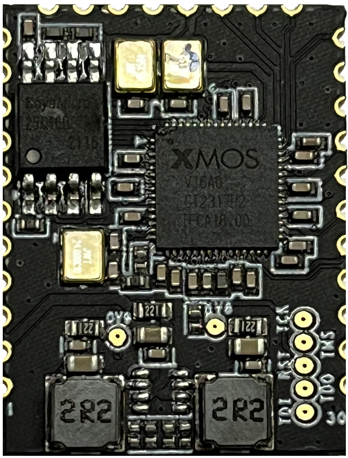
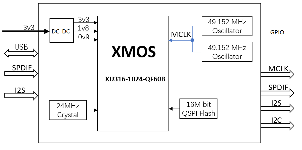
- The A316-1926V1 is a USB multi-channel HD audio decoder module. The module utilizes the XMOS XU316-1024-QF60BC24 chip and integrates high-precision DC-DC chips that output 1.8V and 0.9V voltages to the XU316. The module incorporates 48.152MHz and 49.152MHz active crystals to meet various HD audio sampling rate requirements. The module includes the 24MHz crystal required by the XU316 and a 16Mbit Flash memory for storing audio firmware.
- The A316-1926V1 provides a USB Audio device with USB 2.0 interface compatible with both full-speed and high-speed modes. In USB 2.0 asynchronous mode, it supports sampling rates up to 768 KHz.
- With different firmware configurations, the A316-1926V1 can process up to 6 channels of S/PDIF HD audio and 2 channels of I2S HD audio signals, meeting the requirements of various HD audio decoders.
1.2 Product Features
- USB Interface Features
- USB 2.0 (Full-speed and High-speed)
- USB Audio Class 1.0
- USB Audio Class 2.0
- USB Firmware Upgrade (DFU)
- USB Midi Device Class 1.0
- Supported Audio Protocols
- I2S/TDM
- S/PDIF (Optical/Coaxial)
- Direct Stream Digital (DSD)
- ADAT
- Supported Audio Sampling Rates
- PCM: 44.1kHz, 48kHz, 88.2kHz, 96kHz, 176.4kHz, 192kHz, 352.8kHz, 384kHz, 705.6kHz, 768KHz
- DSD: DSD 64, DSD 128, DSD 256, DSD 512
- DOP: DOP 64, DOP 128, DOP256
- System Compatibility
- UAC 2.0 protocol, supports ASIO, compatible with multiple operating systems including Windows, Linux, Android, macOS, and iOS
1.3 Product Block Diagram
1.4 Specification Description
| Specification Item | Description |
|---|---|
| Product Name | A316-1926V1 |
| Product Description | USB Multi-Channel HD Audio Decoder Module |
| Package Type | SMT Castellated Holes |
| Environmental Statement | All hardware components fully comply with EU RoHS directive |
1.5 Absolute Maximum Ratings
| Parameter | Min | Max | Unit |
|---|---|---|---|
| Storage Temperature | -40 | 125 | ℃ |
| Supply Voltage | -0.5 | 3.63 | V |
| ESD Voltage (Human Body Model) TAMB-25℃ | -2 | 2 | KV |
| ESD Voltage (Machine Model) TAMB-25℃ | -500 | 500 | V |
1.6 Recommended Operating Conditions
| Parameter | Min | Typ | Max | Unit |
|---|---|---|---|---|
| Operating Temperature | 0 | - | 70 | ℃ |
| Operating Voltage | 3 | 3.3 | 3.6 | V |
1.7 Operating Current
| Operating State | Average | Peak | Unit |
|---|---|---|---|
| Active@3.3V | 120 | 200 | mA |
2. Pin Definition
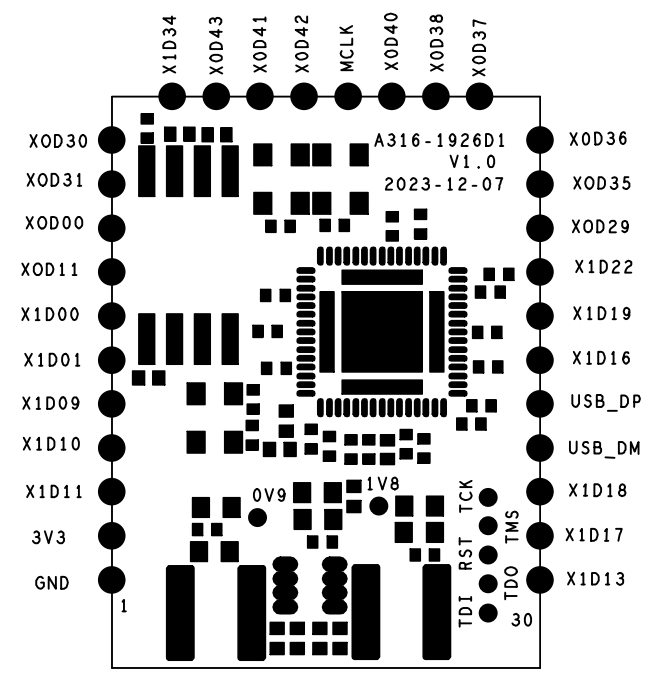
2.1 Pin Layout
2.2 Pin Description
| Module Pin Number | Name | Type | Function |
|---|---|---|---|
| 1 | GND | P | Module Ground |
| 2 | 3V3 | P | Module 3.3V Power Supply |
| 3 | X1D11 | I/O | Multi-function GPIO, refer to PortMap for specific functions |
| 4 | X1D10 | I/O | Multi-function GPIO, refer to PortMap for specific functions |
| 5 | X1D09 | I/O | Multi-function GPIO, refer to PortMap for specific functions |
| 6 | X1D01 | I/O | Multi-function GPIO, refer to PortMap for specific functions |
| 7 | X1D00 | I/O | Multi-function GPIO, refer to PortMap for specific functions |
| 8 | X0D11 | I/O | Multi-function GPIO, refer to PortMap for specific functions |
| 9 | X0D00 | I/O | Multi-function GPIO, refer to PortMap for specific functions |
| 10 | X0D31 | I/O | Multi-function GPIO, refer to PortMap for specific functions |
| 11 | X0D30 | I/O | Multi-function GPIO, refer to PortMap for specific functions |
| 12 | X1D34 | I/O | Multi-function GPIO, refer to PortMap for specific functions |
| 13 | X0D43 | I/O | Multi-function GPIO, refer to PortMap for specific functions |
| 14 | X0D41 | I/O | Multi-function GPIO, refer to PortMap for specific functions |
| 15 | X0D42 | I/O | Multi-function GPIO, refer to PortMap for specific functions |
| 16 | MCLK | I/O | 49.152/45.1584MHz Clock Output |
| 17 | X0D40 | I/O | Multi-function GPIO, refer to PortMap for specific functions |
| 18 | X0D38 | I/O | Multi-function GPIO, refer to PortMap for specific functions |
| 19 | X0D37 | I/O | Multi-function GPIO, refer to PortMap for specific functions |
| 20 | X0D36 | I/O | Multi-function GPIO, refer to PortMap for specific functions |
| 21 | X0D35 | I/O | Multi-function GPIO, refer to PortMap for specific functions |
| 22 | X0D29 | I/O | Multi-function GPIO, refer to PortMap for specific functions |
| 23 | X1D22 | I/O | Multi-function GPIO, refer to PortMap for specific functions |
| 24 | X1D19 | I/O | Multi-function GPIO, refer to PortMap for specific functions |
| 25 | X1D16 | I/O | Multi-function GPIO, refer to PortMap for specific functions |
| 26 | USB_DP | I/O | USB_DP |
| 27 | USB_DM | I/O | USB_DM |
| 28 | X1D18 | I/O | Multi-function GPIO, refer to PortMap for specific functions |
| 29 | X1D17 | I/O | Multi-function GPIO, refer to PortMap for specific functions |
| 30 | X1D13 | I/O | Multi-function GPIO, refer to PortMap for specific functions |
3. Module Dimensions and PCB Footprint
3.1 Module Dimensions
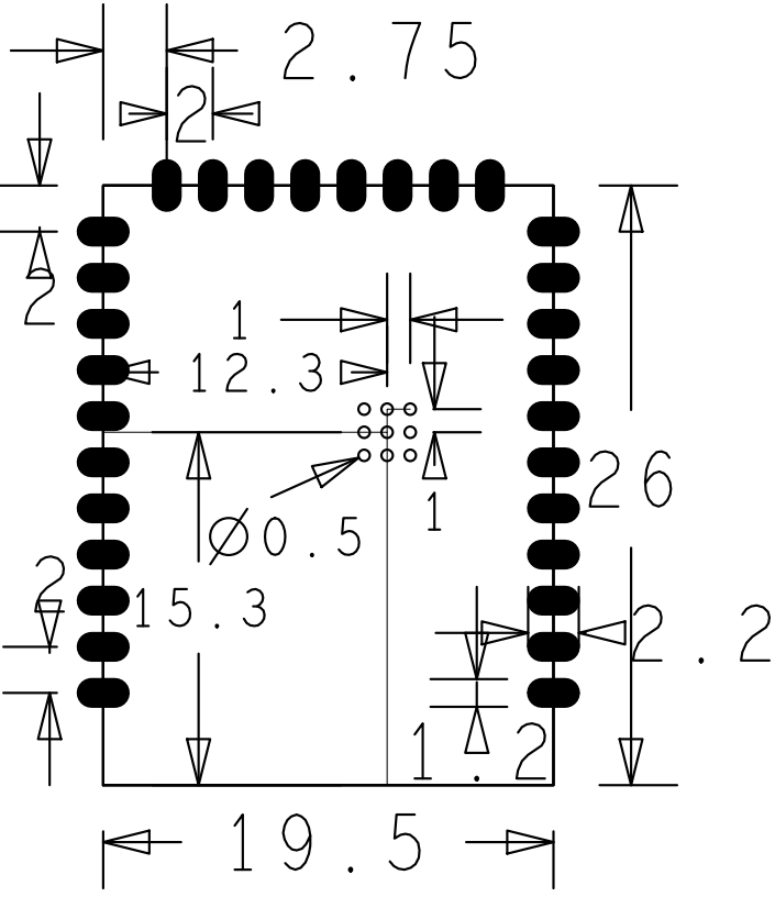
PCB Dimensions: 19.5±0.3(L) × 26±0.3(W) × 0.8±0.1(H)
3.2 Module Footprint
4. Product Packaging Information
Tray + Outer Box Packaging
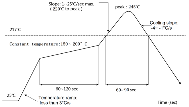
5. Recommended Reflow Soldering Temperature Profile
