OT82111_VC1 Firmware Test Guide
1. Block Diagram Introduction
This guide introduces the test methods and related instructions for OT82111_VC1 firmware on the A316-LS-MIC-V2 evaluation board.
2. A316-LS-MIC-V2 Default Input and A316 Output
- A316-LS-MIC-V2 default input to A316 is fixed at 24-bit 48KHz
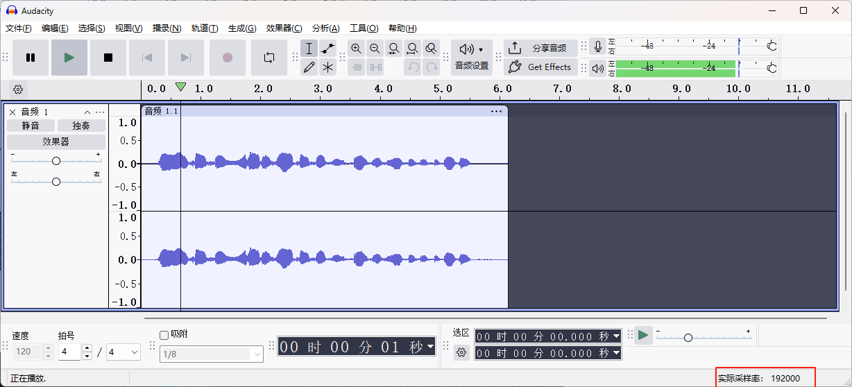
- Regardless of the sampling rate selected during recording, when the USB device outputs to the 3.5mm audio interface (headphone test), the audio will be converted to 24-bit 48KHz for playback
- USB device output to playback device audio format is 24-bit 48KHz and cannot be changed
3. I2S Output Sampling Rate Acquisition and Switching
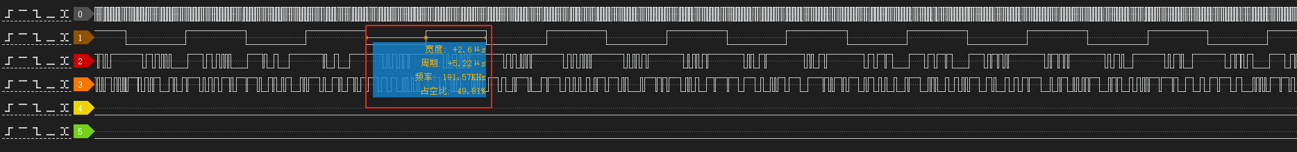
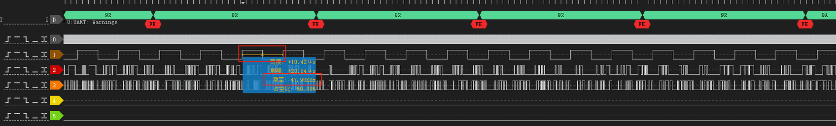
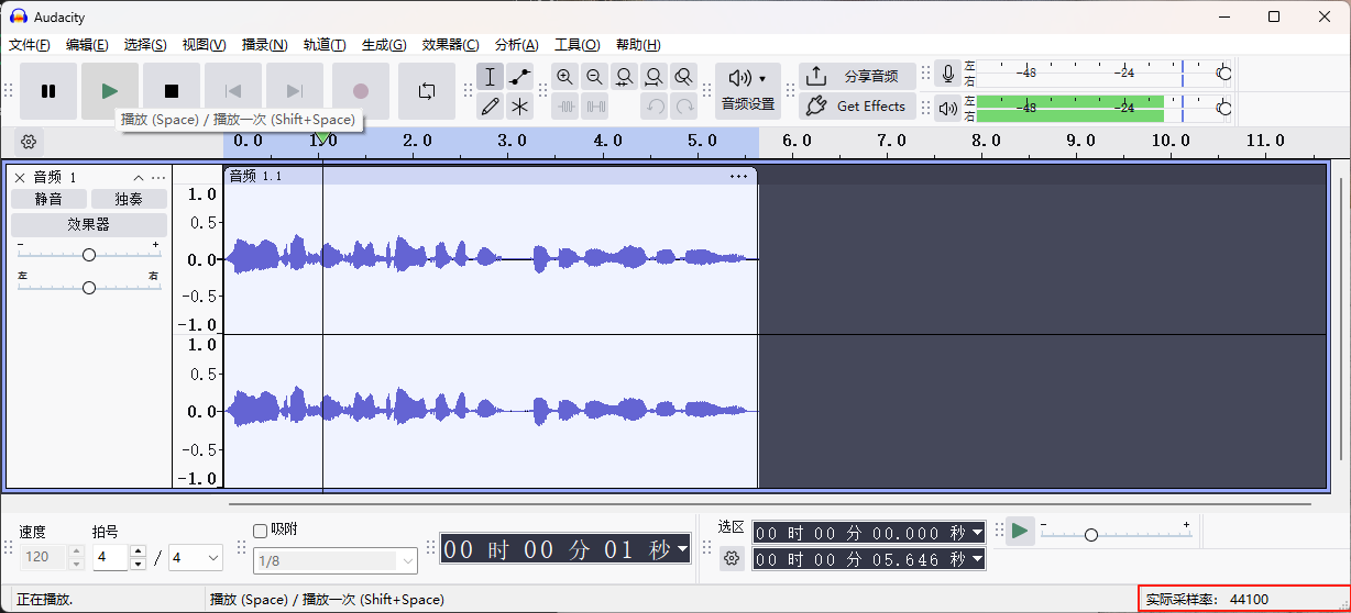
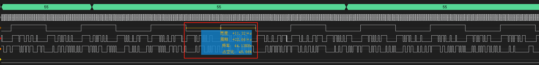
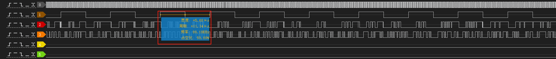
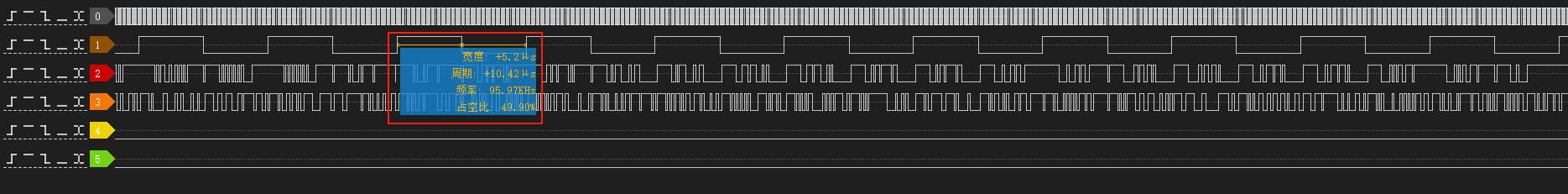
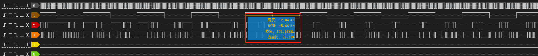
The A316-LS-MIC-V2 evaluation board supports switching between different input sampling rates via button, and audio will be output normally through the 3.5mm interface (headphone test). Switchable sampling rates include: 44.1KHz, 48KHz, 88.2KHz, 96KHz, 176.4KHz, 192KHz. For precise sampling rate measurement, a logic analyzer can be used to capture waveforms (actual measurement may have some error).
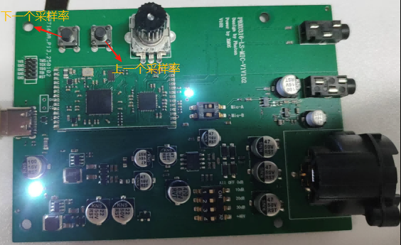
1. Button Location for Switching Sampling Rates
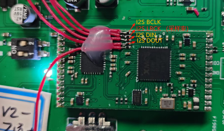
2. A316-LS-MIC-V2 Waveform Capture Connection Method
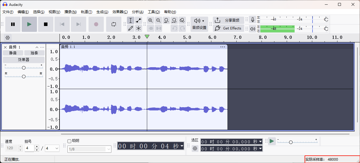
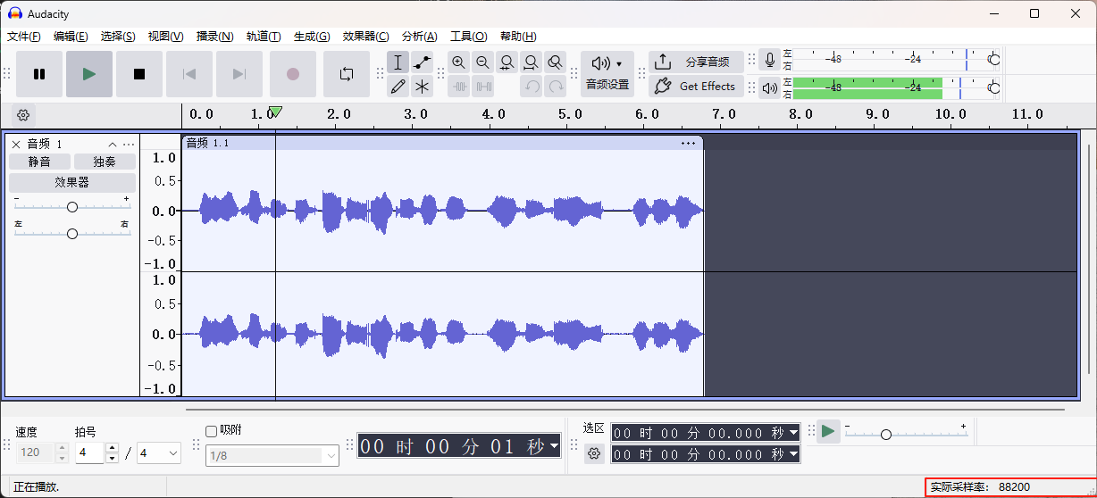
3. Recording and Waveforms at Different Sampling Rates (All 24-bit)
-
44.1KHz:
-
48KHz:

-
88.2KHz:
-
96KHz:

-
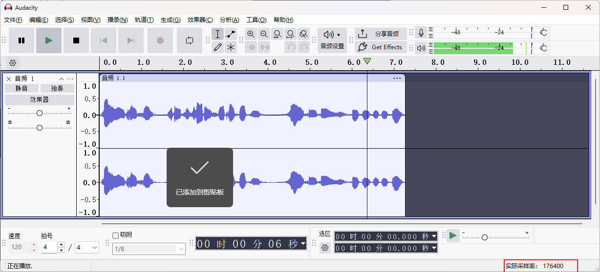
176.4KHz:
-
192KHz: