OT83211-VC1
4-Channel ASRC OTG 44.1KHz~192KHz Audio Sample Rate Converter with Dual I2S Slave Interfaces
1. Introduction
1.1 Product Description
OT83211-VC1 is a high-performance 4-channel ASRC audio sample rate converter designed for mobile audio devices, integrating USB OTG interface and dual I²S slave interface functionality. Based on XMOS high-performance chips, this product is specifically optimized for applications such as live streaming sound cards and mobile audio interfaces.
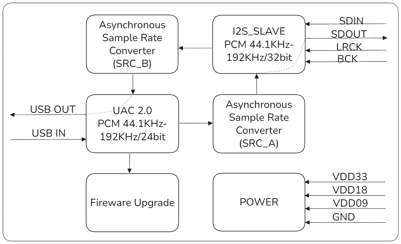
- The product features two built-in high-precision independent dual-channel ASRC sample rate converters, supporting sample rate conversion between 44.1kHz~192kHz, ensuring seamless audio signal conversion between different sample rates.
- Through the USB OTG interface, the device can connect directly to smartphones, tablets, and other mobile devices, utilizing UAC 2.0 for plug-and-play functionality, compatible with Windows, Linux, Android, macOS, iOS and various platforms.
- The product delivers outstanding audio performance specifications with THD+N less than -130dB and SNR greater than 135dB, providing audio equipment manufacturers with professional-grade audio processing solutions.
1.2 Product Features
Audio Performance Features
- Exceptional Audio Quality
- THD+N < -130dB, SNR > 135dB
- ASRC supports conversion between 44.1kHz~192kHz
- Dynamic range ≥110dB, professional-grade audio performance
- 4-Channel ASRC
- Built-in 2 independent dual-channel ASRC
- Can simultaneously process 2-channel upstream and 2-channel downstream ASRC conversion
- Supports I²S Slave mode audio interface
USB Interface Features
- Supports UAC 2.0
- Supports firmware upgrade via USB
- Supports OTG connection
System Compatibility
- Supports multiple operating systems including Windows, Linux, Android, macOS, and iOS
- No special driver installation required
1.3 Application Scenarios
-
Mobile Phone Accompaniment/Live Streaming
- Play background music through phone OTG while performing audio processing. Provides low-latency, high-fidelity audio experience
-
Car Audio Players
- Connect phone to car audio player via USB and play music through the car audio system
1.4 Product Function Block Diagram

1.5 Ordering Information
| PRODUCT MODEL | ORDERING NUMBER | PACKAGE BODY | SIZE (NOM) | Hardware Model | Comments |
|---|---|---|---|---|---|
| OT83211 | OT83211-VC1 | SMT LGA-52 | 13x13mm | A316-Mini-V1 | 4-Channel ASRC OTG 44.1KHz~192KHz Audio Sample Rate Converter with Dual I2S Slave Interfaces |
2. Modes and Specifications
2.1 Supported Input/Output Modes
| Mode Number | Input/Output Mode | Description |
|---|---|---|
| 1 | USB(UAC2.0) ←→I²S(SLAVE) | Supports bidirectional data input/output between USB and I²S(Slave) with internal ASRC conversion |
2.2 Detailed Parameters for Each Operating Mode
2.2.1 USB(UAC2.0) ←→ I²S(SLAVE) Mode
Input/Output Parameters:
| Parameter | Input/Output | Input/Output |
|---|---|---|
| Interface | USB Audio Class 2.0 | I²S(Slave) |
| Audio Format | PCM | PCM |
| Sample Rate | 44.1kHz~192kHz | 44.1kHz~192kHz |
| Bit Depth | Fixed 24bit | Fixed 32bit |
Clock Characteristics:
- I²S interface operates in Slave mode, requiring external BCLK and LRCK signals
- Supports 44.1kHz and 48kHz series sample rates (i.e., 44.1kHz, 88.2kHz, 176.4kHz and 48kHz, 96kHz, 192kHz)
- Supports automatic clock detection and matching
Audio Performance Specifications:
- THD+N < -130dB
- SNR > 135dB
3. Pin Configuration and Functions
3.1 OT83211-VC1 Pin Layout

3.2 OT83211-VC1 Pin Description
| Pin Number | Name | Type | Function |
|---|---|---|---|
| 1 | 3.3V | P | Module 3.3V power supply |
| 2 | X1D13 | I/O | NC |
| 3 | X1D16 | I/O | NC |
| 4 | GND | P | Module ground |
| 5 | X1D17 | I/O | NC |
| 6 | X1D18 | I/O | NC |
| 7 | X1D19 | I/O | NC |
| 8 | X1D22 | I/O | NC |
| 9 | X0D29 | I/O | NC |
| 10 | X0D35 | I | I²S_IN_SCLK(SLAVE) |
| 11 | X0D36 | I | I²S_IN_LRCLK(SLAVE) |
| 12 | X0D37 | I/O | I²S_IN_DATA0(SLAVE) |
| 13 | X0D38 | O | I²S_OUT_DATA0(SLAVE) |
| 14 | X0D40 | I/O | NC |
| 15 | X0D39 | I | XU316 clock input, connected to X1D11 |
| 16 | X0D42 | I/O | NC |
| 17 | X0D41 | I/O | NC |
| 18 | X0D43 | I/O | NC |
| 19 | X1D34 | I/O | NC |
| 20 | GND | P | Module ground |
| 21 | X0D30 | I/O | NC |
| 22 | X0D31 | I/O | NC |
| 23 | X0D32 | I/O | NC |
| 24 | X0D33 | I/O | NC |
| 25 | GND | P | Module ground |
| 26 | GND | P | Module ground |
| 27 | GND | P | Module ground |
| 28 | X0D00 | I/O | NC |
| 29 | X0D11 | I/O | NC |
| 30 | X1D00 | I/O | NC |
| 31 | X1D01 | I/O | NC |
| 32 | GND | P | Module ground |
| 33 | X1D09 | I/O | NC |
| 34 | X1D10 | I/O | NC |
| 35 | X1D11 | I/O | XU316 internal clock output, connected to X0D39 |
| 36 | GND | P | Module ground |
| 37 | GND | P | Module ground |
| 38 | TDI | I/O | XTAG debug PIN |
| 39 | TDO | I/O | XTAG debug PIN |
| 40 | TMS | I/O | XTAG debug PIN |
| 41 | TCK | I/O | XTAG debug PIN |
| 42 | RST_N | I/O | System reset, active low |
| 43 | 1.8V | P | Module 1.8V power supply |
| 44 | GND | P | Module ground |
| 45 | USB_DM | I/O | USB_DM |
| 46 | USB_DP | I/O | USB_DP |
| 47 | GND | P | Module ground |
| 48 | 0.9V | P | Module 0.9V power supply |
| 49 | GND | P | Module ground |
| 50 | GND | P | Module ground |
| 51 | GND | P | Module ground |
| 52 | GND | P | Module ground |
Pin Type Description
I/O type definitions in the table: I=Input, O=Output, P=Power, I/O=Input/Output
4. Hardware Parameters
4.1 Normal Operating Conditions
| Function | Minimum | Typical | Maximum | Unit |
|---|---|---|---|---|
| Operating Temperature | 0 | - | 70 | ℃ |
| 3.3V Operating Voltage | 3.0 | 3.3 | 3.6 | V |
| 1.8V Operating Voltage | 1.62 | 1.80 | 1.98 | V |
| 0.9V Operating Voltage | 0.855 | 0.90 | 0.945 | V |
4.2 Product Dimensions
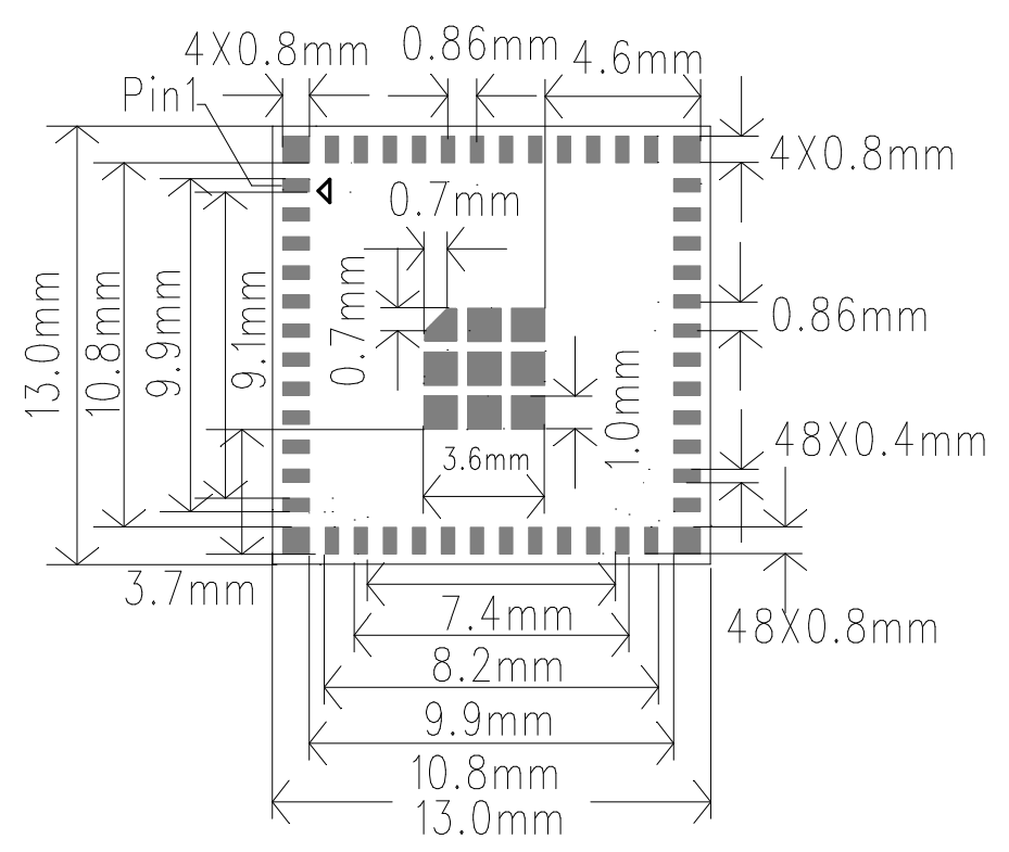
13±0.1mm(L)X13±0.1mm(W)X0.8±0.1mm(H)
4.3 Module Package Diagram

5 Product Packaging Information
Tray + Outer Box Packaging
6. Revision History
| Version | Date | Description | Revised By |
|---|---|---|---|
| V1.0 | 2025-08-10 | Initial version release | |

