XMSRC4192-VC1
2-Channel 192KHz ASRC Audio Sample Rate Converter with 2x S/PDIF and 2x I2S Interfaces
1. Introduction
1.1 Product Description
XMSRC4192 is a high-performance 2-channel asynchronous sample rate converter based on the XMOS chip architecture, providing a wide-range sample rate conversion from 16:1 to 1:16, 144dB dynamic range, and comprehensive support for multiple digital audio formats including I2S, Left-justified, and Right-justified.
- This product integrates two S/PDIF input interfaces, providing users with more flexible signal source selection. Users can flexibly switch between I2S input and S/PDIF input according to application requirements, significantly enhancing system connectivity and adaptability.
- The XMOS chip architecture ensures high reliability and excellent audio processing performance, providing professional audio equipment manufacturers with a more competitive solution.
- Single SRC module architecture capable of simultaneously processing 2-channel audio sample rate conversion.
1.2 Product Features
-
Dual-Channel SRC Audio Sample Rate Conversion
- Single SRC Module Architecture
- Process 2 audio signals (stereo)
- Configurable input sources
- Simultaneous 2-channel audio sample rate conversion
- Flexible Signal Routing
- Input options: I2S_IN or S/PDIF_I
- Output options: I2S_OUT or S/PDIF_O
- Support for multiple operation modes
- Single SRC Module Architecture
-
Ultra-High Sample Rate Conversion Support
- ASRC (Asynchronous Sample Rate Conversion)
- Support sample rate conversion from 44.1KHz to 192KHz
- Support wide-range input/output sample rate ratio from 16:1 to 1:16
- Automatic input/output sample rate detection
- Audio Data Processing
- Support 16bit/24bit/32bit audio data processing
- 144dB dynamic range
- THD+N: -140dB
- ASRC (Asynchronous Sample Rate Conversion)
-
Multi-Interface Support
- S/PDIF Interface
- 2 S/PDIF input/output interfaces (S/PDIF_I, S/PDIF_O)
- Compatible with AES3, IEC 60958, and EIAJ CP-1201 standards
- I²S Interface
- 2 I²S interfaces (1 input + 1 output)
- Support Master/Slave mode
- S/PDIF Interface
-
Comprehensive Digital Audio Format Support
- Support I2S, Left-Justified, Right-Justified formats
- Support 16bit/24bit/32bit audio data processing
- All output data dithered from internal 28-bit data path
-
Flexible Configuration Interface
- I²C/UART Configuration Interface
- Support both I²C and UART dual-protocol configuration
- Configurable Parameters
- Input/output mode
- I²S sample rate configuration (Master mode)
- Master/Slave mode switching
- I²S audio format (I²S/Left-Justified/Right-Justified)
- I²C/UART Configuration Interface
-
Intelligent Clock Management
- Master Clock Output (MCLK)
- Support 128fs, 256fs, 512fs, 1024fs reference clocks
- Master Clock Output (MCLK)
1.3 Application Scenarios
-
Professional Recording Studios
- High-precision sample rate conversion in stereo recording equipment
- Processing audio materials with different sample rates in audio workstations
- Achieving unified audio signal formats in mixing console systems
-
Broadcasting and Television
- Real-time audio signal processing in broadcast equipment
- Synchronous processing of audio from different sources in TV production
- Optimized audio signal conversion in live broadcasting systems
-
Digital Audio Systems
- Audio signal preprocessing in amplifier equipment
- Stereo signal conversion in audio processors
- Signal optimization in speaker management systems
-
Automotive Audio
- Audio format conversion in in-vehicle entertainment systems
- Audio quality optimization processing in high-end audio systems
- Signal processing in noise reduction systems
-
Consumer Electronics
- Audio signal processing in high-end audio equipment
- Stereo processing in home theater systems
- Signal conversion in professional audio interfaces
-
Industrial Applications
- Signal standardization in audio test equipment
- Data processing in audio analysis instruments
- Format conversion in professional signal processing equipment
1.4 Product Block Diagram

1.5 Ordering Information
| PRODUCT MODEL | ORDERING NUMBER | PACKAGE BODY | SIZE (NOM) | Hardware Model | Comments |
|---|---|---|---|---|---|
| XMSRC4192-VC1 | XMSRC4192-VC1 | SMT LGA-52 | 13x13mm | A316-Mini-V1 | 2-channel 192KHz ASRC sample rate converter, single SRC module, 2x S/PDIF inputs |
2. Modes and Specifications
2.1 Supported Input/Output Modes
XMSRC4192-VC1 adopts a single SRC module design with configurable input sources. The following lists typical application modes:
| Mode Number | Input/Output Mode | Description |
|---|---|---|
| 1 | S/PDIF_I → SRC → I²S_OUT (Master) | S/PDIF_I to I²S output |
| 2 | S/PDIF_I → SRC → I²S_OUT (Slave) | S/PDIF_I to I²S output |
| 3 | I²S_IN (Master) → SRC → S/PDIF_O | I²S output to S/PDIF_O output |
| 4 | I²S_IN (Slave) → SRC → S/PDIF_O | I²S output to S/PDIF_O output |
| 5 | I²S_IN (Master) → SRC → I²S_OUT (Master) | Stereo sample rate conversion |
| 6 | I²S_IN (Slave) → SRC → I²S_OUT (Master) | Stereo sample rate conversion |
| 7 | S/PDIF_I → SRC → S/PDIF_O | S/PDIF_I to S/PDIF_O output |
Mode Configuration Instructions
- Configuration can be dynamically switched through I²C/UART interface
2.2 Audio Performance Specifications
| Performance Indicator | ASRC Mode | Test Conditions |
|---|---|---|
| Resolution | 16-32 bits | - |
| Input Sampling Frequency | 44.1kHz ~ 192kHz | - |
| Output Sampling Frequency | 44.1kHz ~ 192kHz | - |
| Dynamic Range | 144dB | -60dBFS input, A-weighted |
| THD+N | -140dB | 0dBFS input, 20Hz~fs/2 |
3. Pin Configuration and Functions
3.1 XMSRC4192_VC1 Pin Layout

3.2 XMSRC4192_VC1 Pin Description
| Pin Number | Name | Type | Function |
|---|---|---|---|
| 1 | 3.3V | P | Module 3.3V power supply |
| 2 | X1D13 | I | S/PDIF_B (S/PDIF output) |
| 3 | X1D16 | - | Reserved |
| 4 | GND | P | Module ground |
| 5 | X1D17 | - | Reserved |
| 6 | X1D18 | - | Reserved |
| 7 | X1D19 | - | Reserved |
| 8 | X1D22 | - | Reserved |
| 9 | X0D29 | I/O | NC |
| 10 | X0D35 | I/O | BCLKI (I²S input bit clock, Master output/Slave input) |
| 11 | X0D36 | I/O | LRCKI (I²S input frame sync, Master output/Slave input) |
| 12 | X0D37 | I | S/PDIF_I (S/PDIF input) |
| 13 | X0D38 | - | SDIN (I²S data input) |
| 14 | X0D40 | I/O | NC |
| 15 | X0D39 | O | MCLK_OUT (Master clock output) |
| 16 | X0D42 | - | Reserved |
| 17 | X0D41 | I/O | NC |
| 18 | X0D43 | - | Reserved |
| 19 | X1D34 | - | Reserved |
| 20 | GND | P | Module ground |
| 21 | X0D30 | I/O | CTL_MUTE |
| 22 | X0D31 | I/O | UART_I2C_SEL (UART/I2C selection) |
| 23 | X0D32 | I/O | NC |
| 24 | X0D33 | - | Reserved |
| 25 | GND | P | Module ground |
| 26 | GND | P | Module ground |
| 27 | GND | P | Module ground |
| 28 | X0D00 | I | UART_TX/I2C_SCL |
| 29 | X0D11 | O | UART_RX/I2C_SDA |
| 30 | X1D00 | - | LRCKO (I²S output frame sync, Master output/Slave input) |
| 31 | X1D01 | - | SDOUT (I²S data output) |
| 32 | GND | P | Module ground |
| 33 | X1D09 | - | Reserved |
| 34 | X1D10 | - | BCLKO (I²S output bit clock, Master output/Slave input) |
| 35 | X1D11 | O | MCLK_OUT (Master clock output) |
| 36 | GND | P | Module ground |
| 37 | GND | P | Module ground |
| 38 | TDI | I/O | JTAG debug interface |
| 39 | TDO | I/O | JTAG debug interface |
| 40 | TMS | I/O | JTAG debug interface |
| 41 | TCK | I/O | JTAG debug interface |
| 42 | RST_N | I | System reset, active low |
| 43 | 1.8V | P | Module 1.8V power supply |
| 44 | GND | P | Module ground |
| 45 | USB_DM | I/O | USB_DM (Reserved, not used) |
| 46 | USB_DP | I/O | USB_DP (Reserved, not used) |
| 47 | GND | P | Module ground |
| 48 | 0.9V | P | Module 0.9V power supply |
| 49 | GND | P | Module ground |
| 50 | GND | P | Module ground |
| 51 | GND | P | Module ground |
| 52 | GND | P | Module ground |
Pin Type Definitions
I/O types in the table: I=Input, O=Output, P=Power, I/O=Input/Output
Important Notes
- UART/I2C Interface Selection: Select interface type through pin 22 (X0D31) UART_I2C_SEL signal
- MCLK Output: Pin 15 (X0D39) and pin 35 (X1D11)
- Required for Master mode, supports 128fs/256fs/512fs/1024fs
4. Configuration Interface Description
4.1 I²C/UART Configuration Interface
XMSRC4192-VC1 supports both I²C and UART dual-protocol configuration, providing flexible configuration options. The UART_I2C_SEL signal on pin 22 (X0D31) can be used to select which configuration interface to use:
| Configuration Method | Pin 22 (X0D31) | Communication Interface | Description |
|---|---|---|---|
| Pull-up | UART_I2C_SEL | UART Mode | Pin 29 (X0D11)=UART_RX, Pin 28 (X0D01)=UART_TX |
| Pull-down | UART_I2C_SEL | I²C Mode | Pin 29 (X0D11)=I2C_SDA, Pin 28 (X0D01)=I2C_SCL |
4.2 Configurable Parameters
The following parameters can be configured through I²C or UART interface:
| Parameter Type | Configuration Options | Description |
|---|---|---|
| Input/Output Mode | Select from 7 input/output modes | |
| I²S Sample Rate | 4kHz~192kHz | Configured in Master mode |
| I²S Input Format | I²S/Left-Justified/Right-Justified | Audio data format |
| I²S Output Format | I²S/Left-Justified/Right-Justified | Audio data format |
| Output Word Length | 16/24/32 bits |
Configuration Instructions
- For detailed configuration commands, please refer to the configuration protocol documentation
4.3 MCLK Configuration
- Master mode ports require MCLK for generating LRCK and BCK
- MCLK supports 128fs/256fs/512fs/1024fs
5. Hardware Parameters
5.1 Normal Operating Conditions
| Function | Minimum | Typical | Maximum | Unit |
|---|---|---|---|---|
| Operating Temperature | 0 | - | 70 | ℃ |
| 3.3V Operating Voltage | 3.0 | 3.3 | 3.6 | V |
| 1.8V Operating Voltage | 1.62 | 1.80 | 1.98 | V |
| 0.9V Operating Voltage | 0.855 | 0.90 | 0.945 | V |
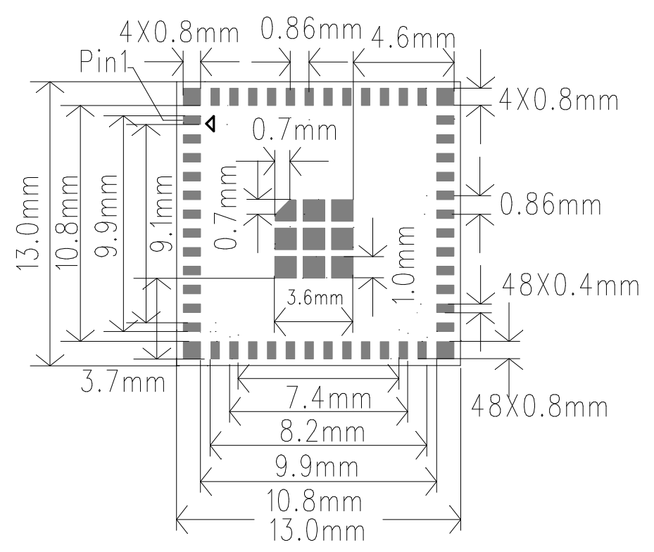
5.2 Product Dimensions
13±0.1mm(L)X13±0.1mm(W)X0.8±0.1mm(H)
5.3 Module Package Diagram

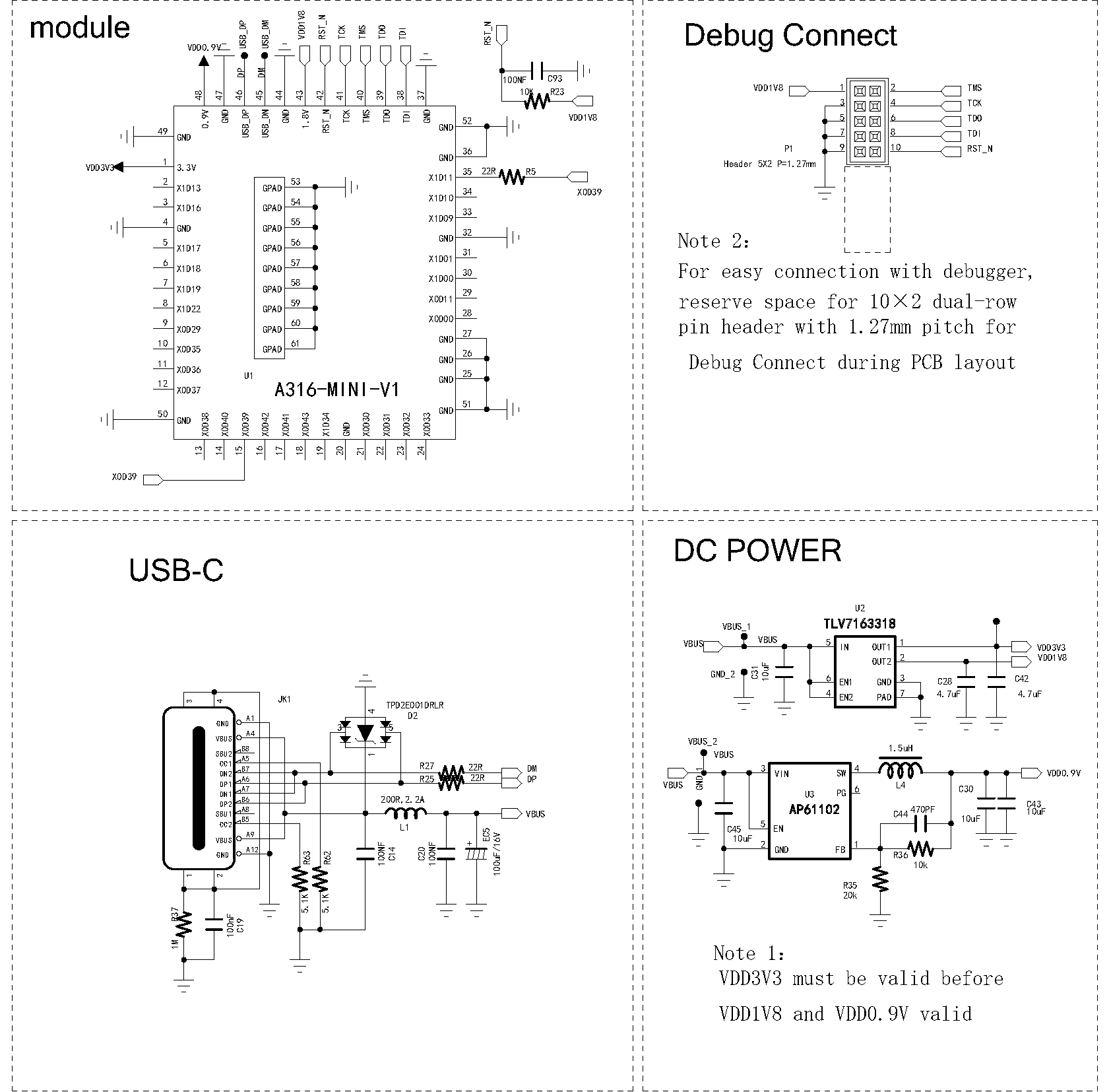
6. Minimum System Reference Design

7. Product Packaging Information
Tray + Outer Box Packaging
8. Revision History
| Version | Date | Description | Revised By |
|---|---|---|---|
| V1.0 | 2025-10-6 | Initial release | Technical Documentation Department |

